
Vous êtes ici : ILVFRPlateformes techniques
- Mis à jour le 21 mars 2024
- Version PDF
CEFS2 (XPS, Nano-Auger, SEM-EDS-EBSD)
Le Centre d'Etudes et de Formation en Spectroscopies Electroniques et de Surface (CEFS2) est dédié à l'analyse de la physico-chimie des surfaces prises dans toutes ses dimensions (haute résolution pour l'étude des environnements chimiques, détection de traces, accès à la distribution de composition chimique en profondeur et dans le plan de la surface, accès à des inhomogénéités jusqu'aux dimensions nanométriques, etc.). Le centre se compose de 3 spectromètres XPS, un spectromètre Nano-Auger et un SEM-FEG-EDX-EBSD.

Un partenariat particulier existe avec l'IPVF. Elle se traduit par l'accueil à temps plein d'un postdoctorant sur le Projet I et l'installation sur le site de l'UFR de l'UVSQ Sciences (site de Versailles), d'une plateforme IPVF dédiée à l'analyse chimique des surfaces (XPS K Alpha+ et GD OES) , avec le fort soutien du CNRS et de l'UVSQ. Cette plateforme IPVF est sous la responsabilité technique (maintenance, mise en œuvre et gestion) des ingénieurs CEFS2.
XPS
Les spectromètres XPS fournissent des informations élémentaires et chimiques sur divers matériaux (solides, poudres, polymères, etc.) avec une résolution latérale de 10 à 600 μm et une profondeur d'analyse inférieure à 10 nm. Des profondeurs plus élevées peuvent être atteintes par profilage par abrasion ionique (mono ou polyatomique). L'analyse angulaire est également possible. La compensation du canon à compensation de charge permet l'étude des matériaux conducteurs mais aussi isolants. Matériaux divers (solides, poudres, polymères...) avec une résolution latérale de 10 à 600 μm et une profondeur d'analyse inférieure à 10 nm.
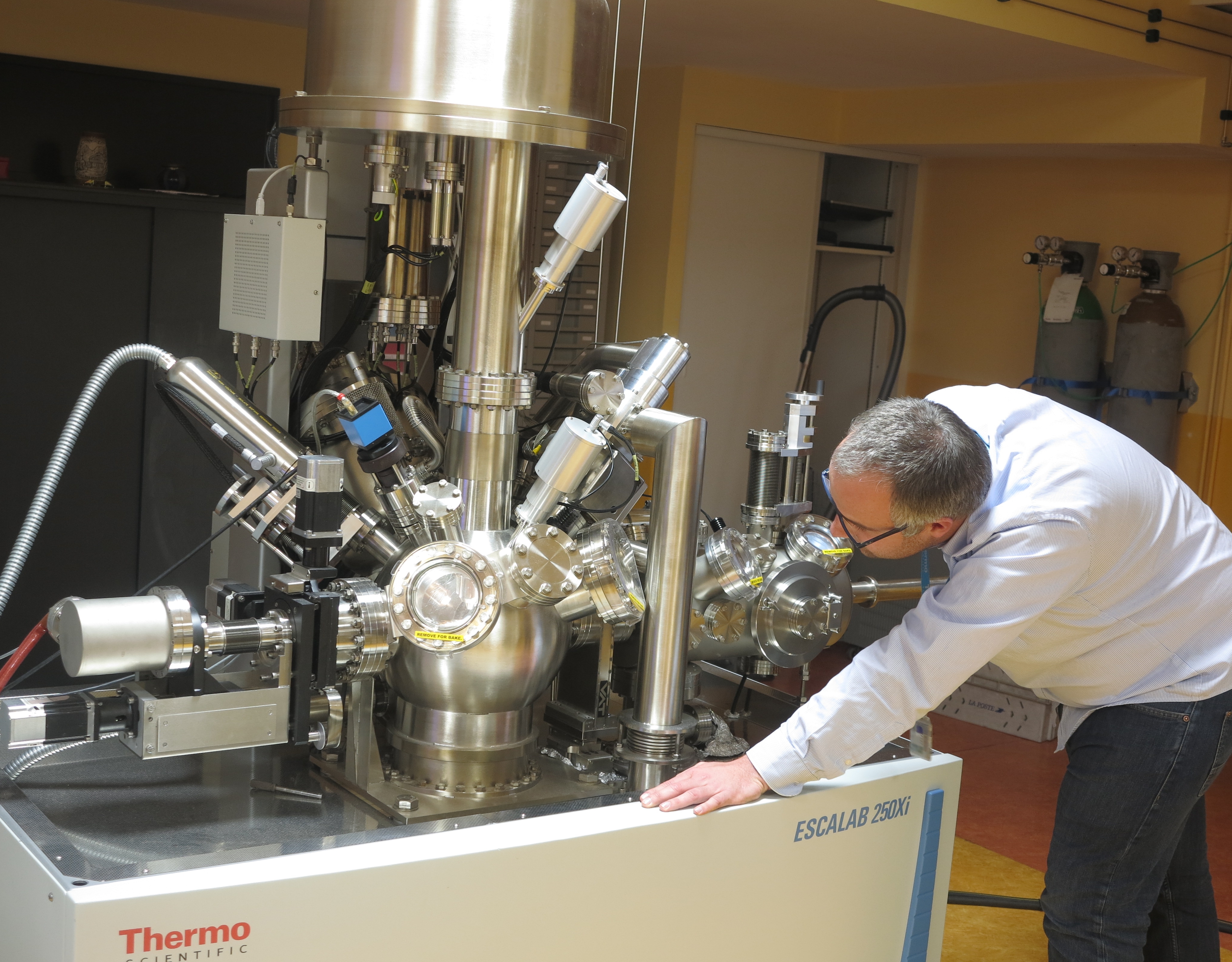
L'Escalabe 250 Xi offre une très haute résolution énergétique. Une lampe à hélium permet des mesures de spectroscopie UV (UPS) donnant accès aux bandes de valence. L'utilisation d'ions légers Hélium permet d'accéder à la composition de la première couche atomique (Low Energy Ion Scattering). Un module REELS (Reflection Electron Energy Loss Spectroscopy) permet d'accéder à l'hydrogène, un élément non sondé par XPS.
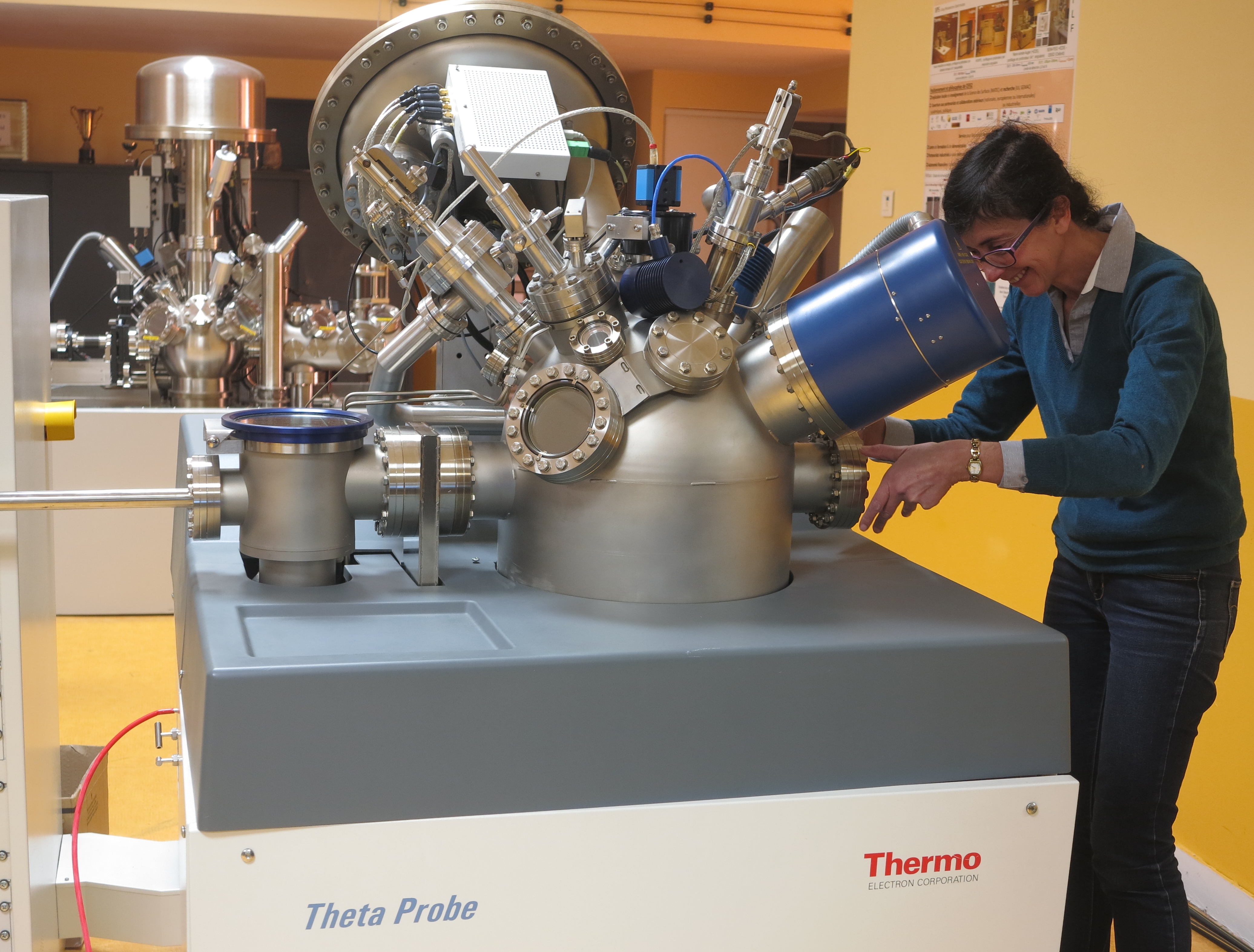
L'appareil Theta Probe permet une analyse dans les premiers nanomètres par résolution angulaire sans déplacer les échantillons.
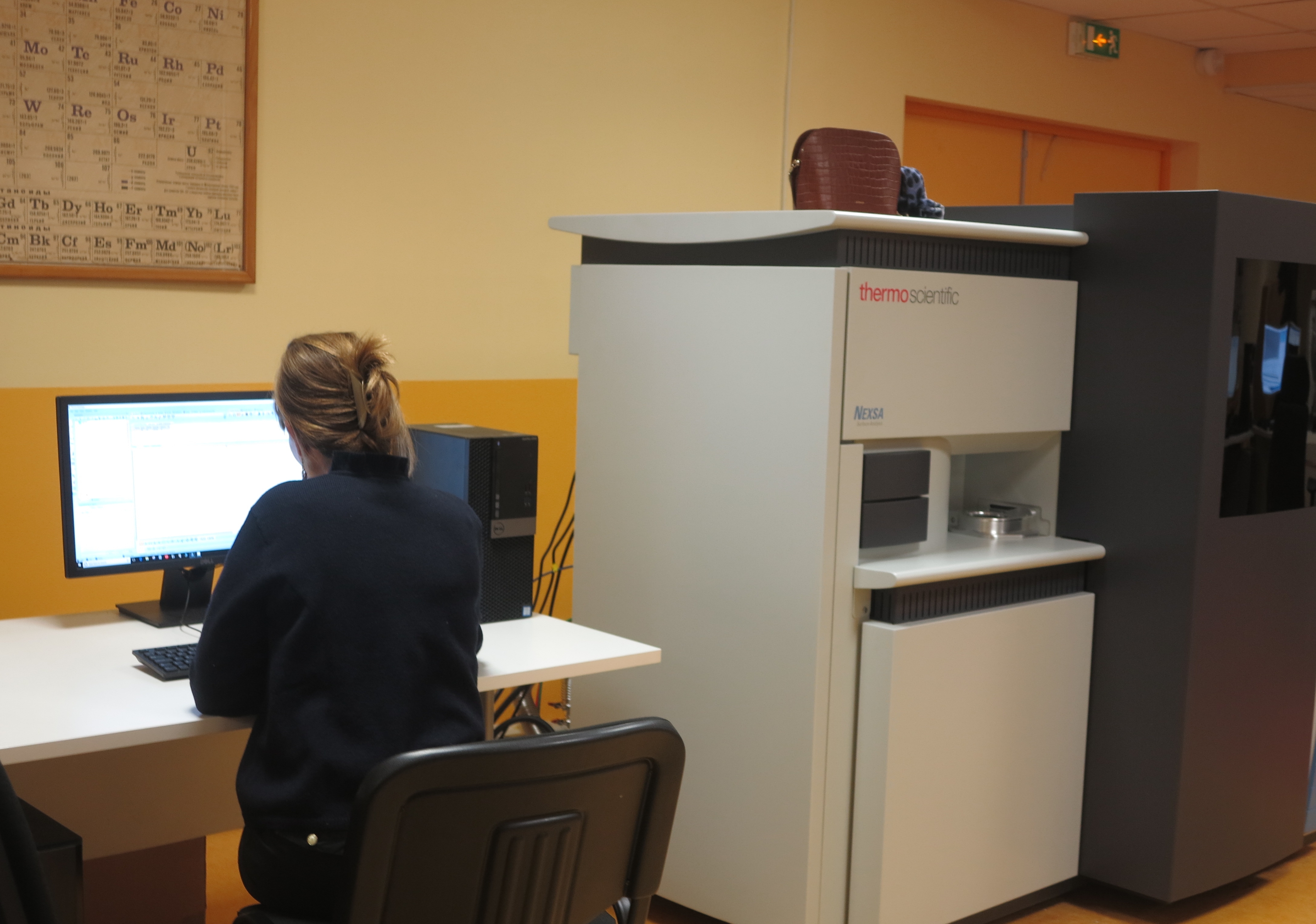
Grâce à sa petite taille de spot, le Nexsa offre une résolution de dix microns donnant accès à des cartes chimiques élémentaires et à des environnements.
L'appareil Theta Probe permet une analyse dans les premiers nanomètres par résolution angulaire sans déplacer les échantillons.
Grâce à sa petite taille de spot, le Nexsa offre une résolution de dix microns donnant accès à des cartes chimiques élémentaires et à des environnements.
Nano-Auger
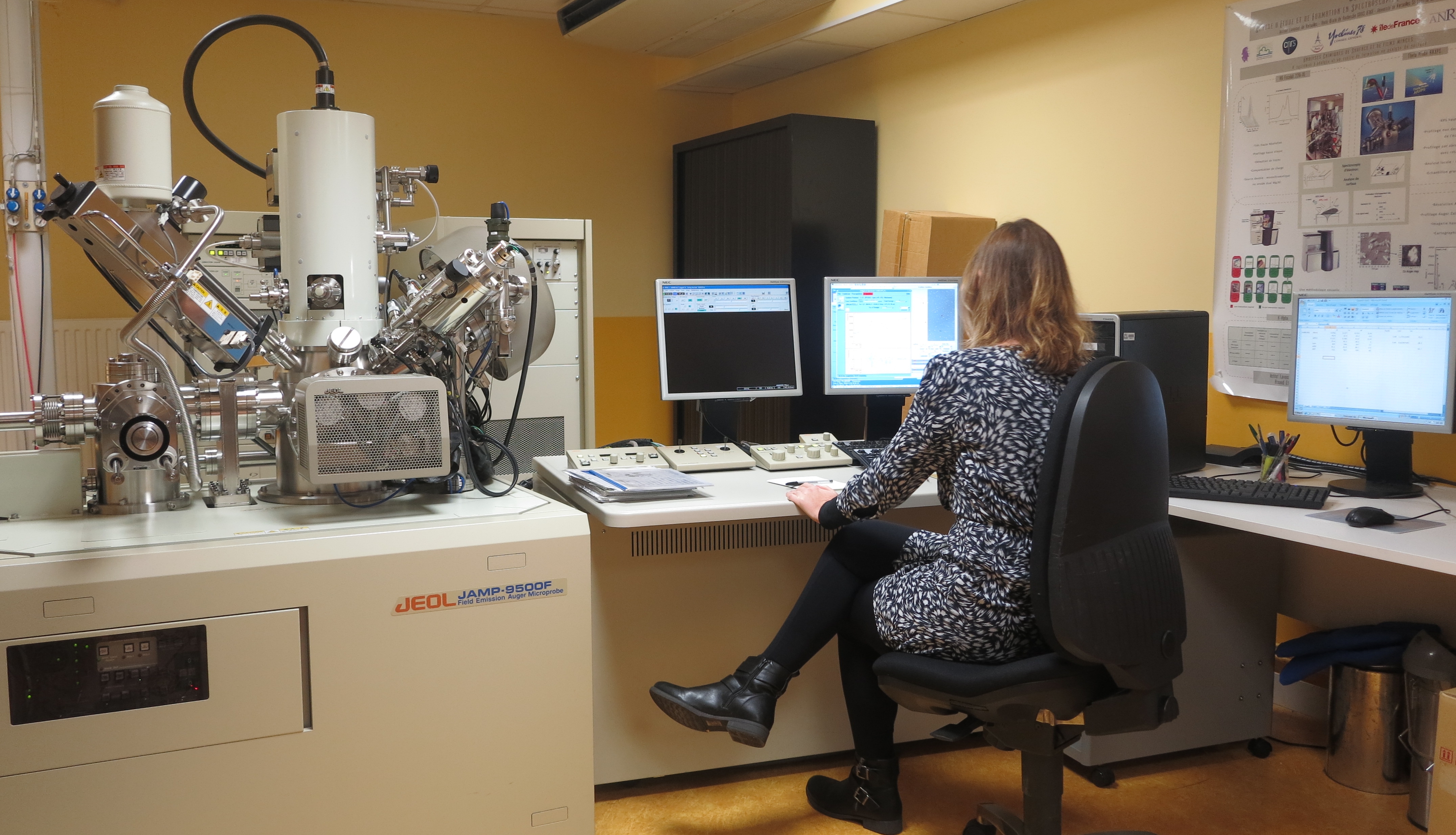
The JAMP 9500 F Nano-AES (+ EDS) spectrometer enables qualitative and quantitative analyzes on essentially conductive materials. Several modes are accessible (points, lines, cartography). The analysis depth is less than 5 nm for a lateral resolution of 10 to a few hundred nanometers. Angular analysis is possible by tilt, in depth by sequential ionic abrasion and by volume by EDS (from Na Z = 11
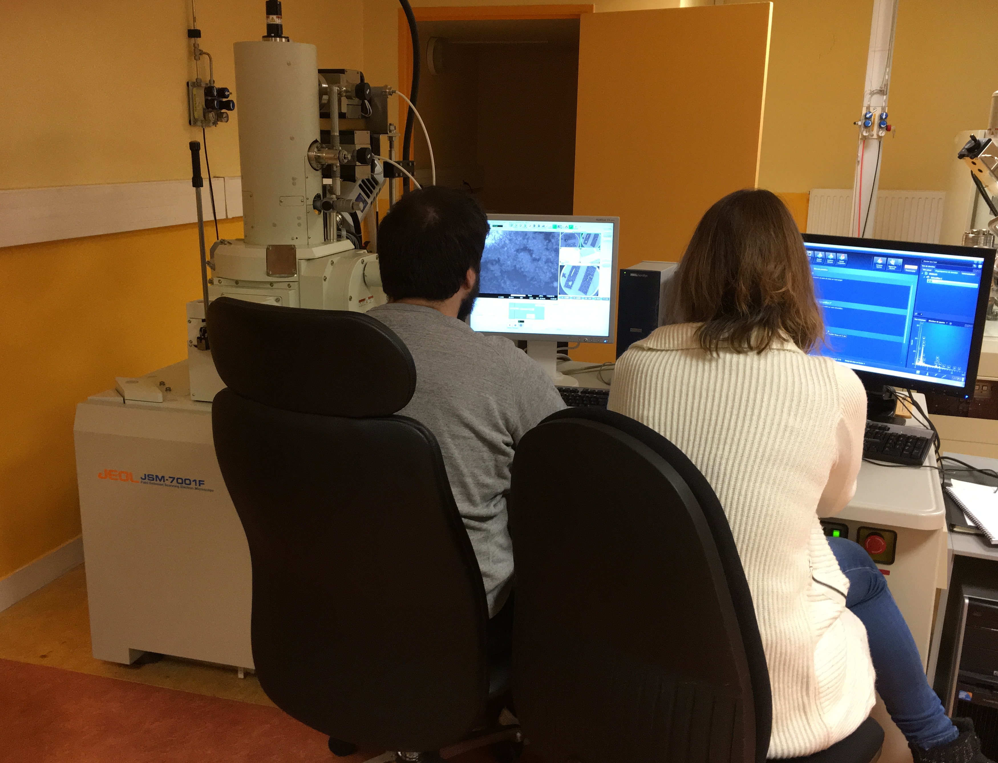
SEM-FEG/EDS et EBSD
The JSM 7001 F microscope is equipped with an EDS detector allowing qualitative and quantitative analyzes on a depth of 300 nm to 2 microns with a micrometric side resolution. Different modes, points, lines and cartography are accessible. It is also equipped with an EBSD module allowing crystallographic analyzes (grain size, orientation, texturing) on polished samples
Centre de formation en spectroscopies d'électrons
Université, CNRS Formation Entreprises