You are here : ILVENResearch TeamsEPIInterfaces and devices
- Updated on August 26, 2024
- PDF version
Interfaces and devices
The fundamental understanding of semiconductor/semiconductor, metal/metal and semiconductor/metal interfaces is a major challenge in optoelectronics devices and in the fields of energy, heritage conservation, etc. The EPI group studies these interfaces by exploring their reactivities on a micro/nanometric scale via their stabilities (corrosion, failure, passivation, etc.). To do this, the optoelectronic properties of the interfaces are studied and modulated by monitoring the surface chemistry on a nanometric scale (XPS, nano Auger probe, etc.), combining (photo)electrochemistry, ion bombardment and accelerated aging. These interfaces can also be modified by selective dissolution in aqueous media or by nanometric metallic and/or semiconductor deposition using (photo)electrochemistry.
Semiconductors passivation
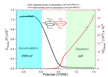
The strong surface reactivity of InP requires a passivation treatment. EPI controls at the nanometric scale by (photo)electrochemical treatment in liquid ammonia (Patm, -55°C) a nitrided film which belongs to polyphosphazene. These researches have been recovered by two patents, 3 international extensions, an ANR (EPINAL 2018-22) and a CNRS 2019 prematuration project, supported by EPI.
Recent publications
Perovskite oxides
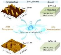 Perovskite oxides (ABO3) are a class of materials of highest interest due to their multiple functional properties. These studies are carried out in collaboration with the FOX team in GEMaC (UVSQ) which is an expert in oxide growth by Pulsed Laser Deposition (PLD). In the case of SrVO3, we evidenced the presence of an over-oxidized layer which is soluble in an aqueous medium (application of sacrificial layers). This work has opened the way to the development of new transparent conductive oxides (TCO).
Recent publications
Chemical engineering
Recent publications
Metallic contacts
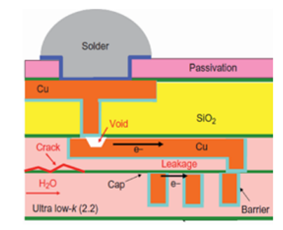
Dans les composants électroniques, les interconnexions métalliques assurent le transport du courant et doivent présenter des résistivités de plus en plus faibles. Ces contraintes imposent une maîtrise parfaite des interfaces à l’échelle nanométrique. EPI étudie la stabilité et la réactivité chimique de films métalliques d’épaisseurs nanométriques (Cu, Co, Ni, …) d’un point de vue fondamental (société Aveni) mais aussi appliquées (société Linxens). In electronic components, metallic interconnections are used to carry current, and must have ever-lower resistivities. These constraints require a perfect control of these interfaces at nanometric scale. EPI studies the stability and chemical reactivity of thin metallic films (Cu, Co, Ni, …) from both fundamental (Aveni company) and applied (Linxens company) approaches.
Aging
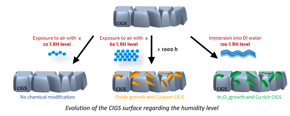
The EPI team is engaged in the study of the aging of solar absorber materials, with a particular focus on the Cu(In,Ga)Se₂ (CIGS) absorber. Using a climatic chamber, the team has identified the various key factors responsible for the reactivity of the CIGS surface, including relative humidity, illumination, temperature, and the nature of the atmosphere. They have also investigated the effects of these factors on the CIGS surface.
Recent publications
HEMT
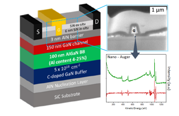
High electron mobility transistors (HEMTs), in particular the GaN sector, are capable of providing increasingly high powers and efficiencies, essential to the development of new communication technologies. The EPI team studies the chemical and structural changes (C2N collaboration) taking place at the interfaces of the devices in order to understand the mechanisms at the origin of drifts in electrical behavior (IEMN collaboration) leading to the failure of these components (DGA GREAT project).
Recent publications
Heritage
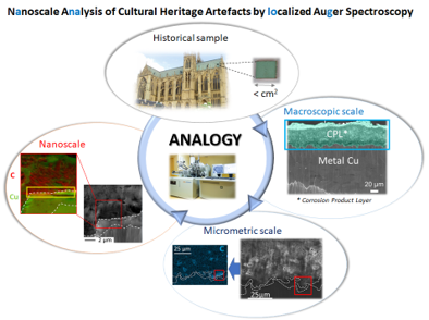
In the case of metallic objects, understanding the formation of layers of corrosion products makes it possible to trace the corrosion mechanisms and to propose actions to preserve these heritage objects. To address this major challenge, our team is studying the nature and interweaving of oxidized phases down to the deca-nanometric scale (nano-Auger), which constitutes important information for the development of new protective treatments (LAPA/NIMBE collaboration).


