
You are here : ILVENFacilitiesCEFS2 PlatformSurface analysis
- Partager cette page :
- PDF version
EN : CEFS2 (XPS, Nano-Auger, SEM-EDS-EBSD)
The Electron Spectroscopies Center provides access to the physico-chemistry of surfaces taken in all its dimensions (high resolution in energy and chemical environment, trace detection, ability to access the distribution of composition perpendicular to the surface, distribution in the plane of the surface, access to inhomogeneity up to nanometric dimensions, etc.). It consists of 3 XPS spectrometers, a Nano-Auger spectrometer and a SEM-FEG-EDX-EBSD.
A physico-chemistry of interfaces partnership exists with IPVF. It is reflected in the full-time reception of a postdoctoral fellow on Project I and the installation on the UFR site of the UVSQ Sciences (Versailles site), of an IPVF platform dedicated to surface chemical analysis (XPS K Alpha + and GD OES), with strong support from CNRS and UVSQ. This IPVF platform is under the technical responsibility (maintenance, implementation and "relay" management) of CEFS2 engineers.
XPS
XPS spectrometers make it possible the determination of elementary and chemical environment of various materials (solids, powders, polymers, etc.) with a lateral resolution of 10 to 600 μm and a depth of analysis of less than 10 nm.
Higher depths are achieved by deep profiling by ionic abrasion (mono or polyatomic). Angular analysis is also possible. Load compensation allows the study of conductive but also insulating materials.
Higher depths are achieved by deep profiling by ionic abrasion (mono or polyatomic). Angular analysis is also possible. Load compensation allows the study of conductive but also insulating materials.
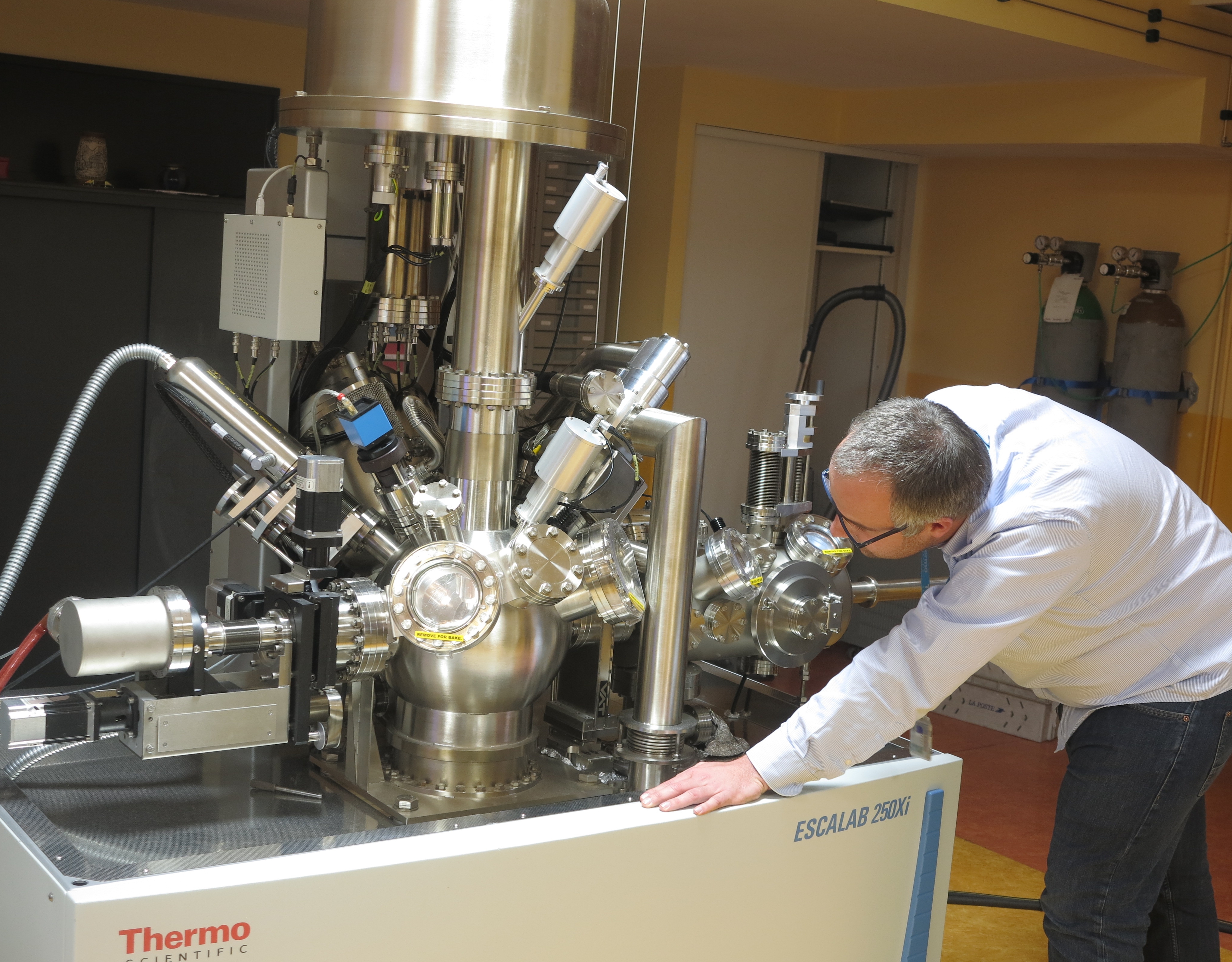
The Escalab 250 Xi device offers a very high energy resolution. A helium lamp allows measurements of UV spectroscopy (UPS) giving access to the valence bands. The use of Helium light ions makes it possible to access the composition of the first atomic layer (Low Energy Ion Scattering). A REELS module (Reflection Electron Energy Loss Spectroscopy) allows in particular to access hydrogen, non-probed element by XPS spectroscopy.
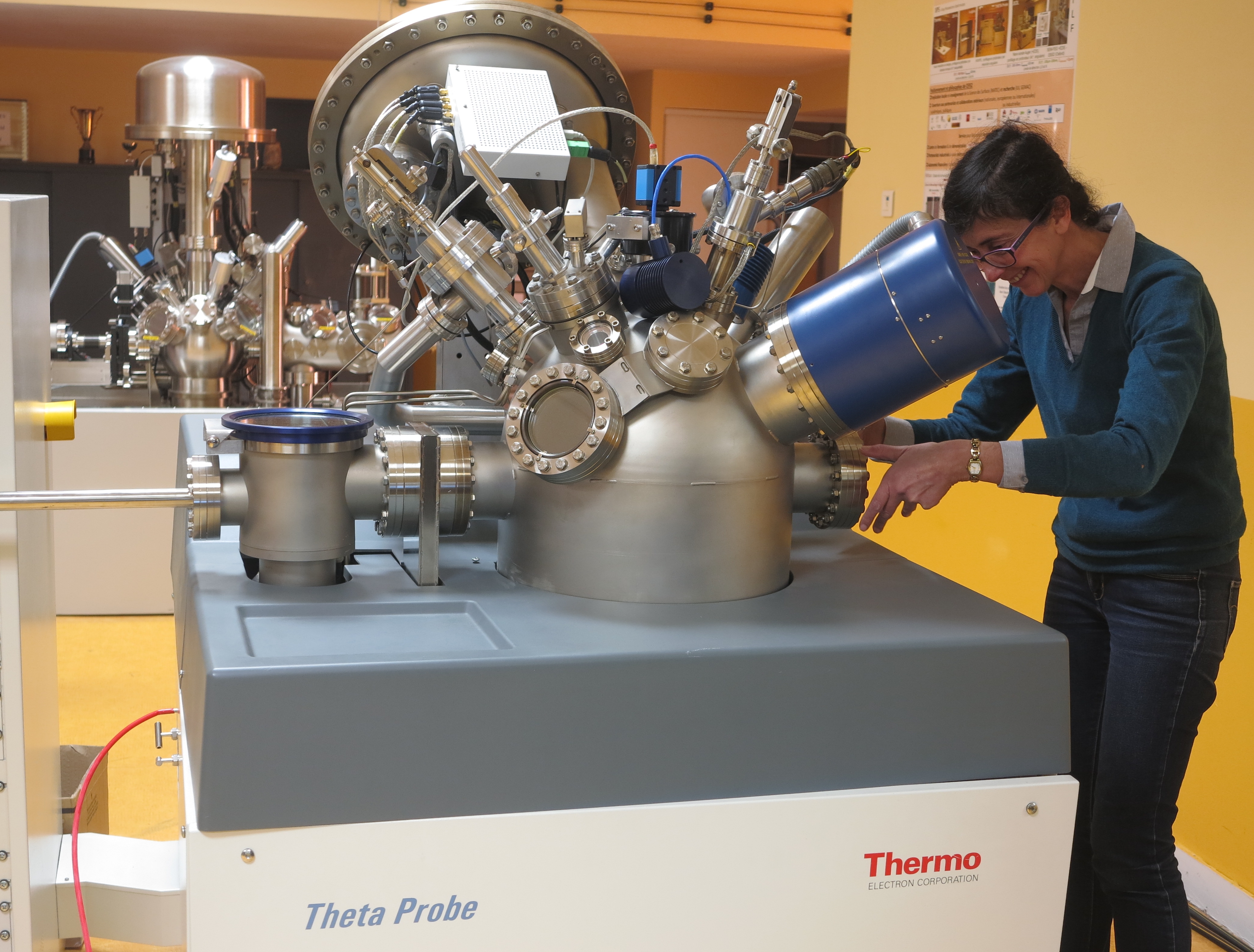
The Theta Probe device allows deep analysis in the first nanometers by angular resolution without tilt.
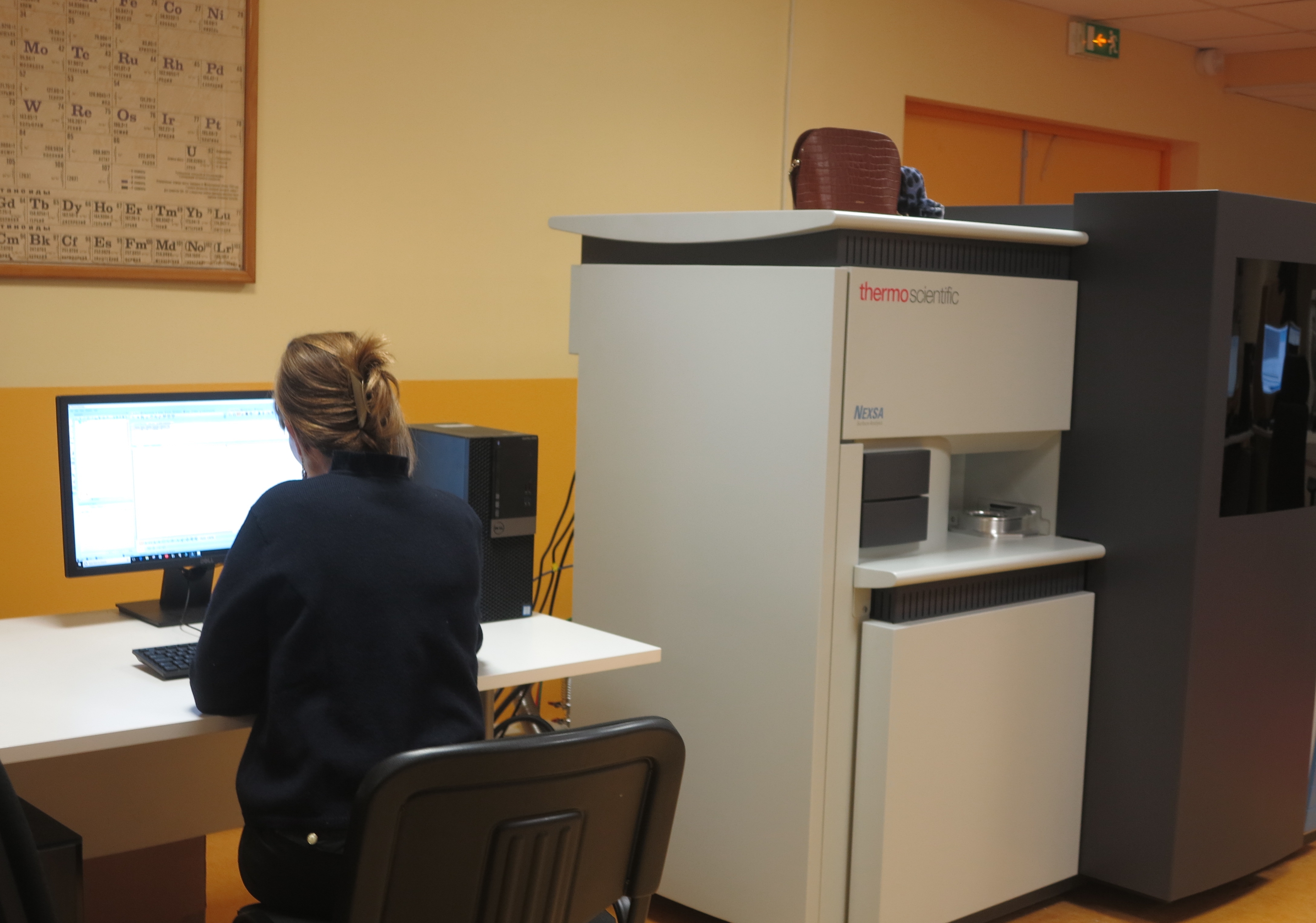
The Nexsa device, thanks to its low spot size, has a resolution of ten microns giving access to elementary chemical maps and environments.
The Theta Probe device allows deep analysis in the first nanometers by angular resolution without tilt.
The Nexsa device, thanks to its low spot size, has a resolution of ten microns giving access to elementary chemical maps and environments.
Nano-Auger
The JAMP 9500 F Nano-AES (+ EDS) spectrometer enables qualitative and quantitative analyzes on essentially conductive materials. Several modes are accessible (pointing, line, cartography). The analysis depth is less than 5 nm for a lateral resolution of 10 to a few hundred nanometers. Angular analysis is possible by tilt, in depth by sequential ionic abrasion and by volume by EDS (from Na Z = 11).

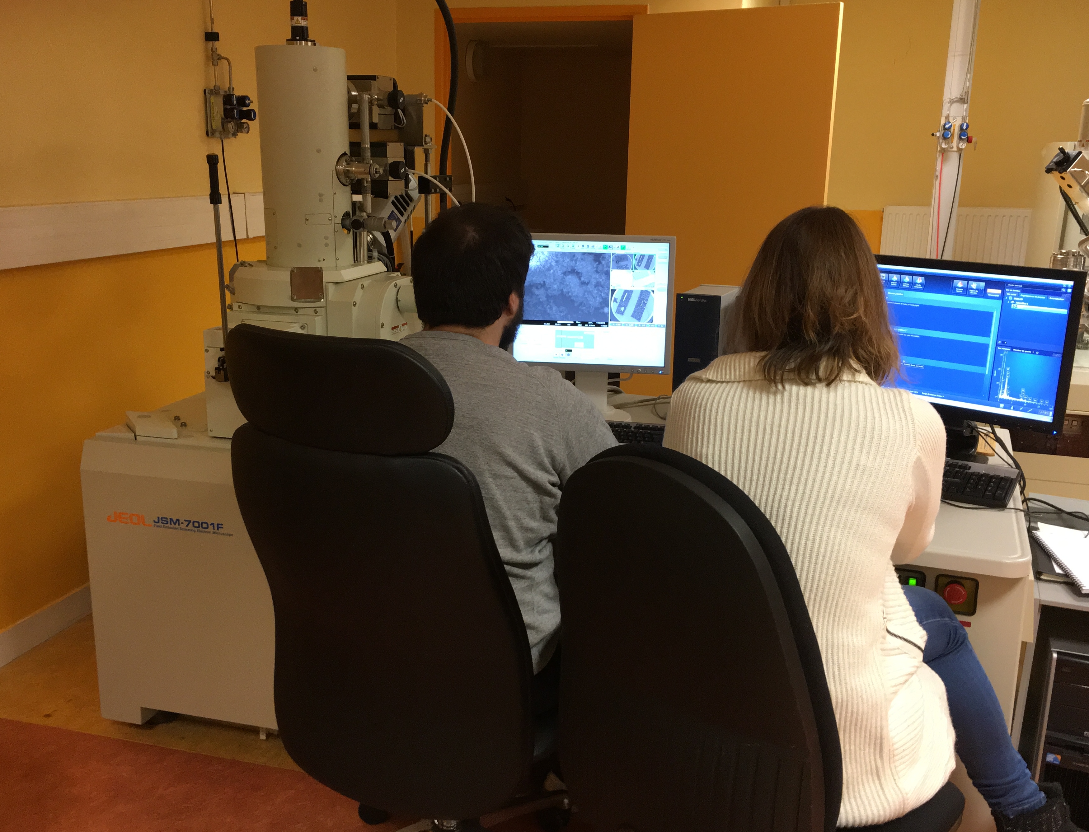
SEM-FEG/EDS and EBSD
The microscope JSM 7001 F is equipped with an EDS detector allowing qualitative and quantitative analyzes on a depth of 300 nm to 2 microns and with a micrometric side resolution. The pointed modes, lines and cartography are accessible. It is also equipped with an EBSD module allowing crystallographic analyzes (grain size, orientation, texturing) on polished samples
Electron Spectroscopy Training Center
University, CNRS, companies, conferences
This center is open to the entire scientific community.
Service managers:
Muriel Bouttemy
Mathieu Frégnaux
Muriel Bouttemy
Mathieu Frégnaux